DRAM Chip Replacement BGA Rework: Full Process from Desoldering to Reflow
2026-04-02 · ResolderWorks
When a DRAM chip fails on a server memory (DDR RAM) module, it leads to memory errors, ECC failures, and even complete system crashes. DRAM chips are mounted using BGA (Ball Grid Array) technology, making them impossible to replace with standard soldering — professional BGA rework equipment and expertise are absolutely required.
Today, ResolderWorks reveals the complete process of our DRAM chip replacement BGA rework in 11 detailed steps.
What is BGA Rework? BGA rework is the precision repair process of removing a BGA-packaged chip from a circuit board and re-mounting a new or functional replacement. With hundreds of solder balls arranged under each DRAM chip, the process demands advanced techniques including reballing, flux application, precision alignment, and controlled reflow.
The Full Repair Process — 11 Detailed Steps
DRAM chip replacement rework follows 11 key stages. From sourcing a donor chip to the final reflow — every one of these steps is required to replace a single chip.
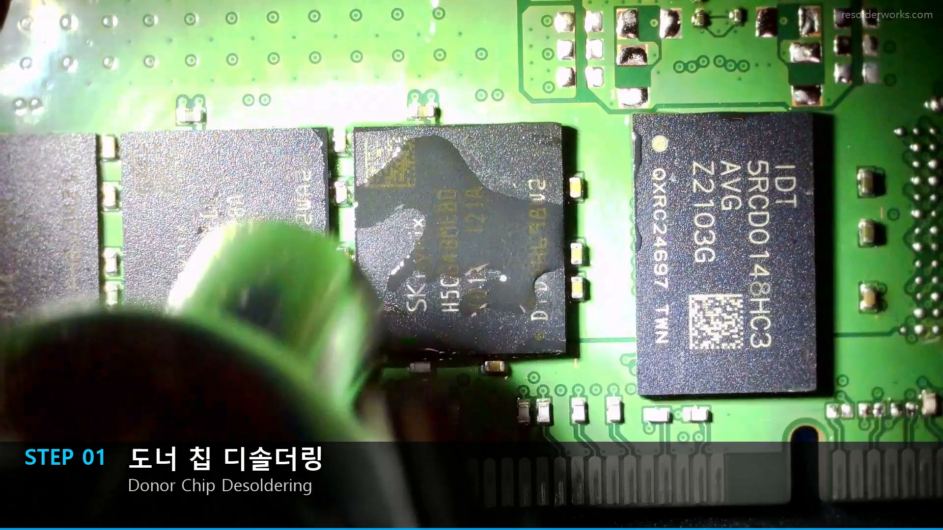
Step 1. Donor Chip Desoldering
To source a functional DRAM chip, we start by desoldering a chip from a donor memory module. Using a hot air gun, we heat the area around the target chip to melt the BGA solder balls.
Temperature management is critical. Overheating can damage the chip, while insufficient heat means the solder won't melt and the chip won't release.
Donor chip desoldering Heating the donor chip's BGA solder balls with a hot air gun
Step 2. Donor Chip Removal
Once the solder is fully melted, we carefully lift the chip using a vacuum pickup tool or tweezers. It's crucial to remove the chip vertically and cleanly to avoid damaging the BGA pads.
[Donor chip removal]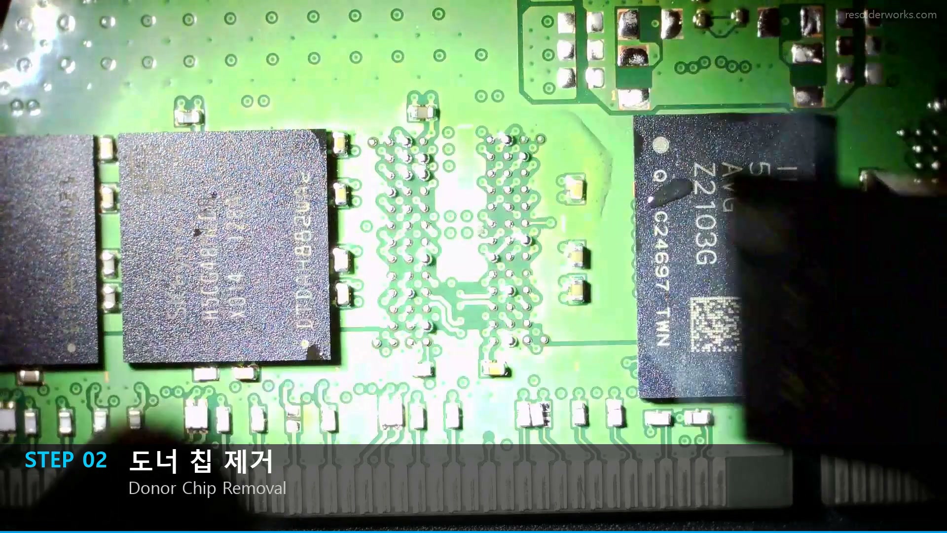 DRAM chip successfully removed from the donor module
Step 3. Damaged Chip Removal
Now we move to the target memory module — the one being repaired. The faulty DRAM chip is heated with a hot air gun and removed from the board.
After removing the damaged chip, we carefully inspect the PCB pads. If any pads are damaged, additional repair work is needed before proceeding.
[Damaged chip removal start]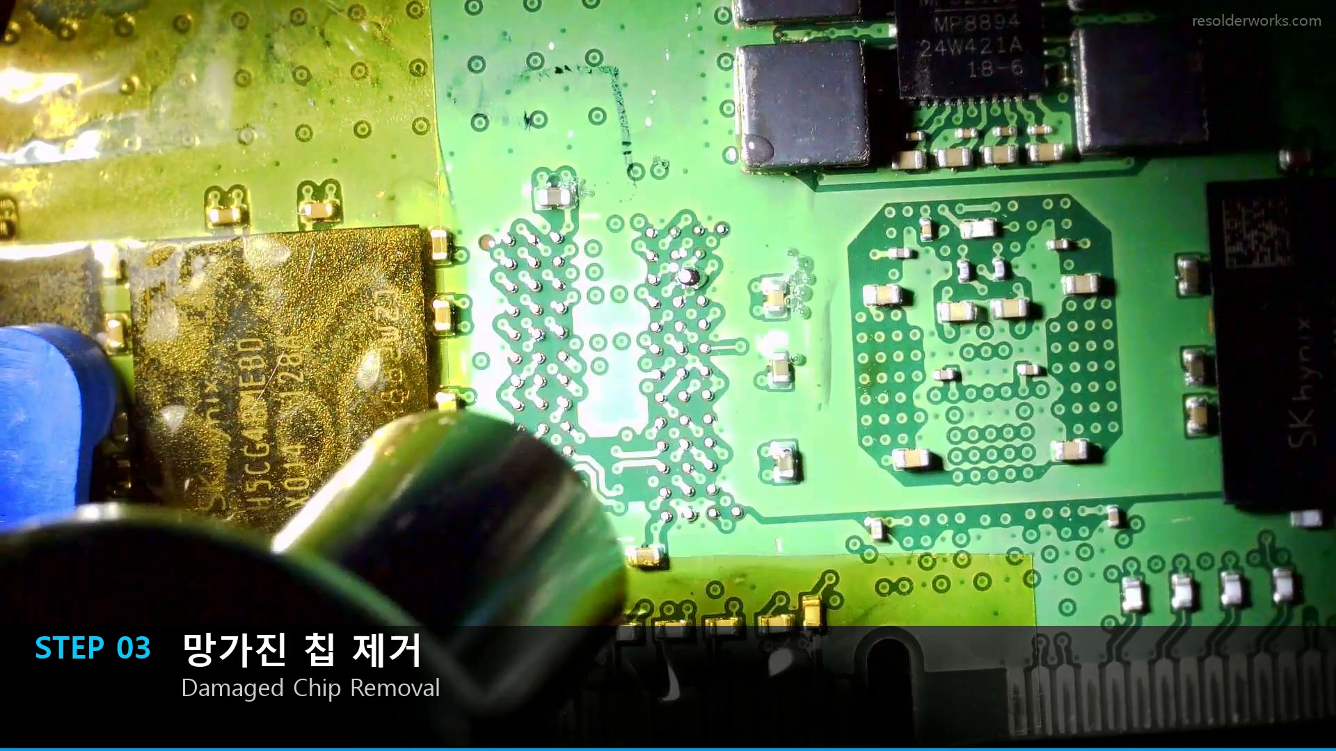 Beginning removal of the faulty DRAM chip
[Damaged chip removal action]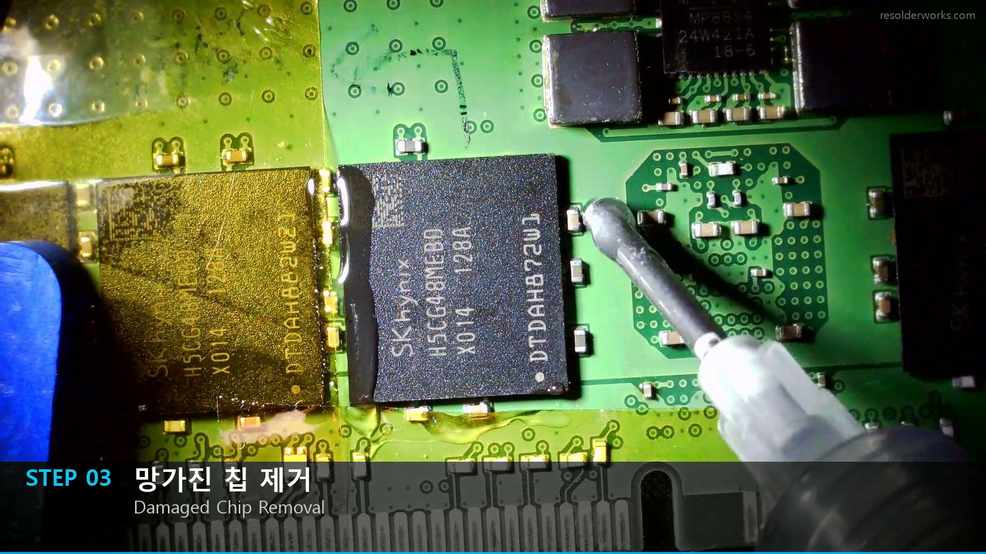 Heating and removing the damaged chip
Step 4. PCB Pad Solder Wicking
After chip removal, residual solder remains unevenly on the PCB pads. We use solder wick and a soldering iron to cleanly remove all leftover solder from the pads.
If this step is done poorly, solder bridges (shorts) can occur when mounting the new chip — so meticulous precision is essential.
[PCB pad solder wicking 1]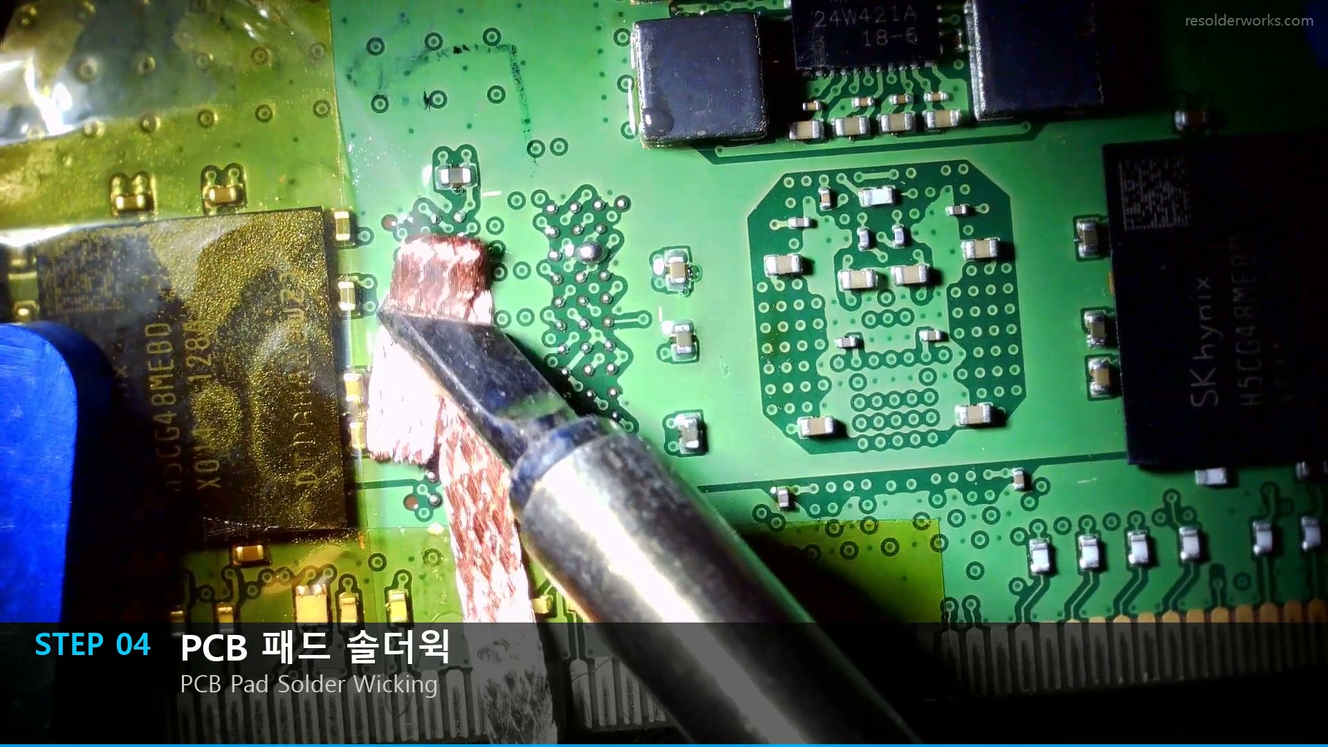 Removing residual solder with solder wick
[PCB pad solder wicking 2]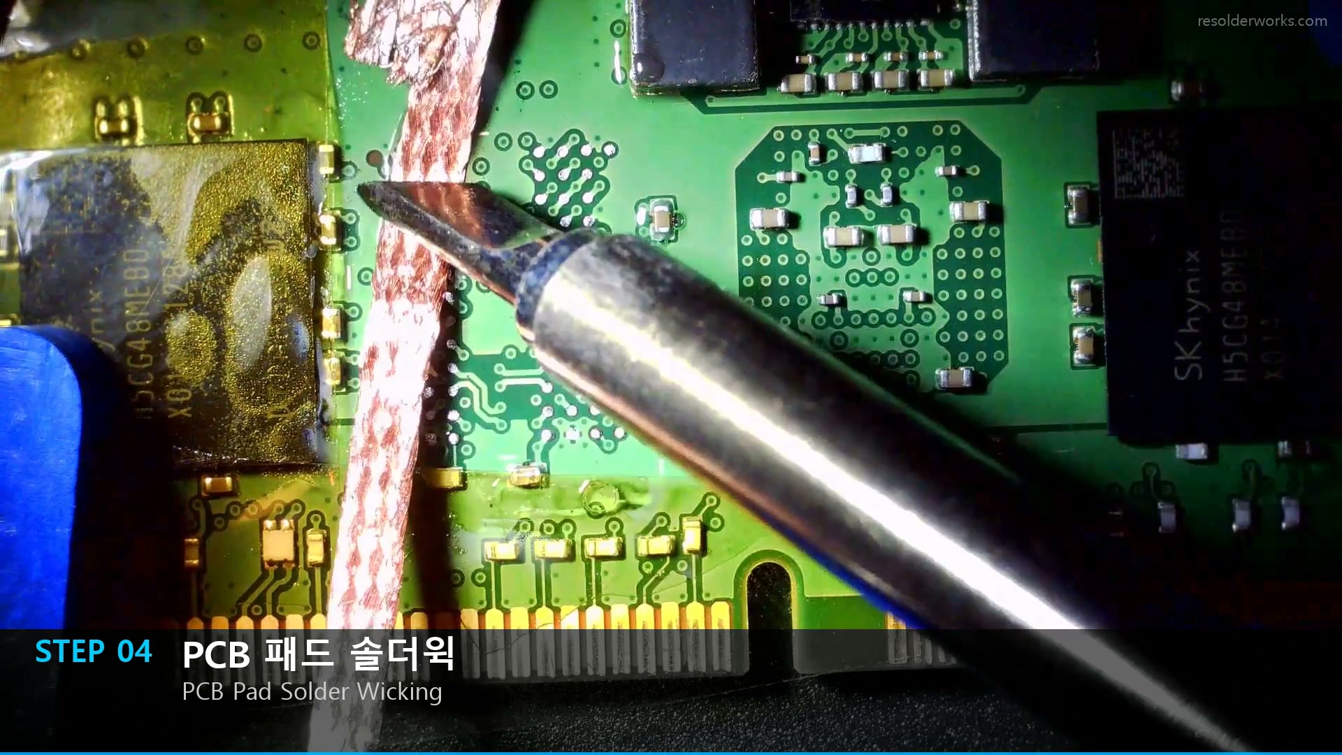 PCB pad solder wicking complete
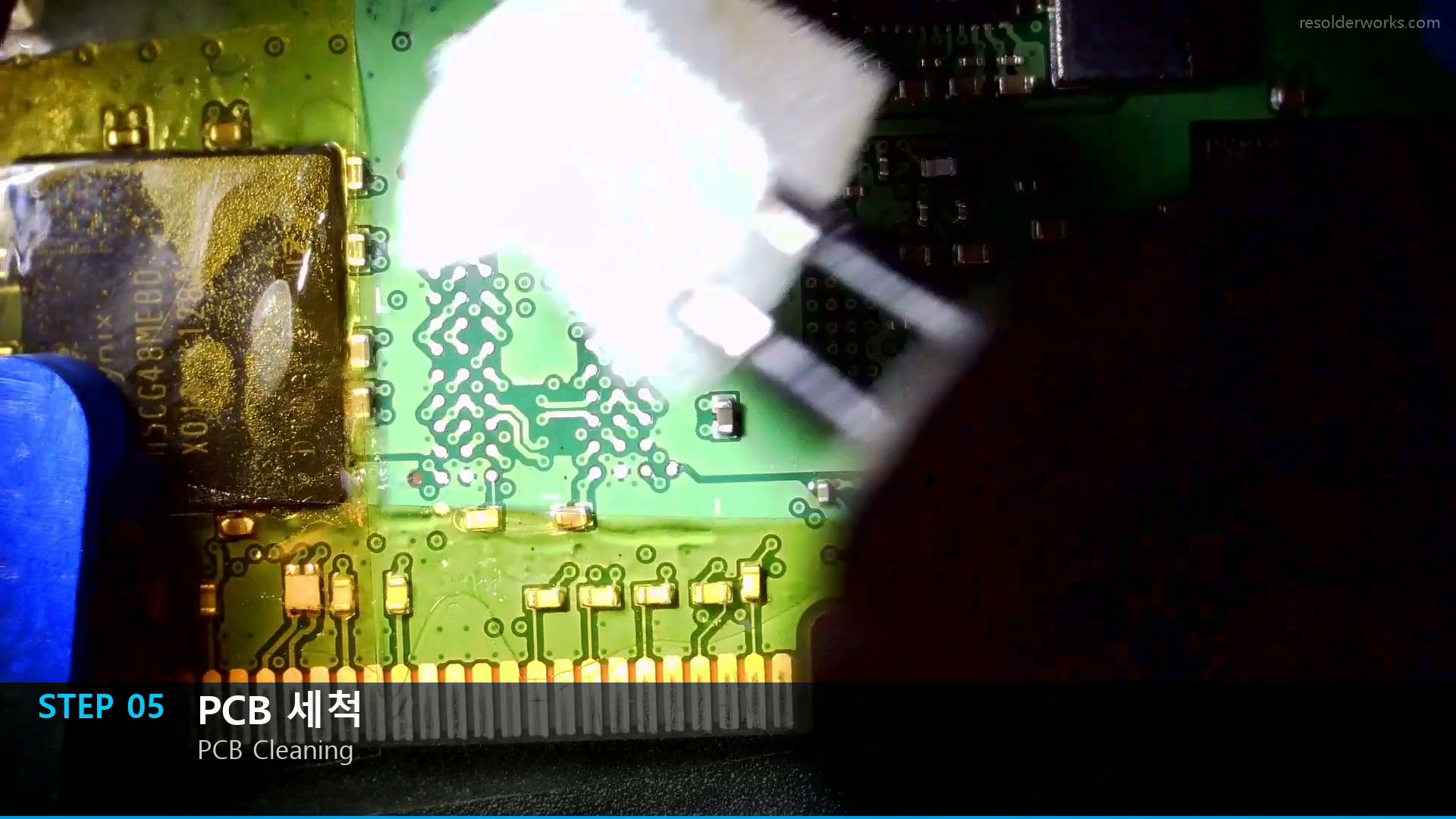
Step 5. PCB Cleaning
After solder wicking, we clean any remaining flux residue and contaminants from around the pads. IPA (isopropyl alcohol) and cotton swabs are used to thoroughly clean the surface.
[PCB cleaning]image Cleaning the PCB pads with IPA
Step 6. Chip Flux Application
We apply flux to the BGA pads on the donor chip. Flux prevents oxidation during soldering and ensures smooth solder flow — it's an essential material for BGA work.
Applying the right amount evenly is key. Too much flux can actually cause defects.
[Chip flux application]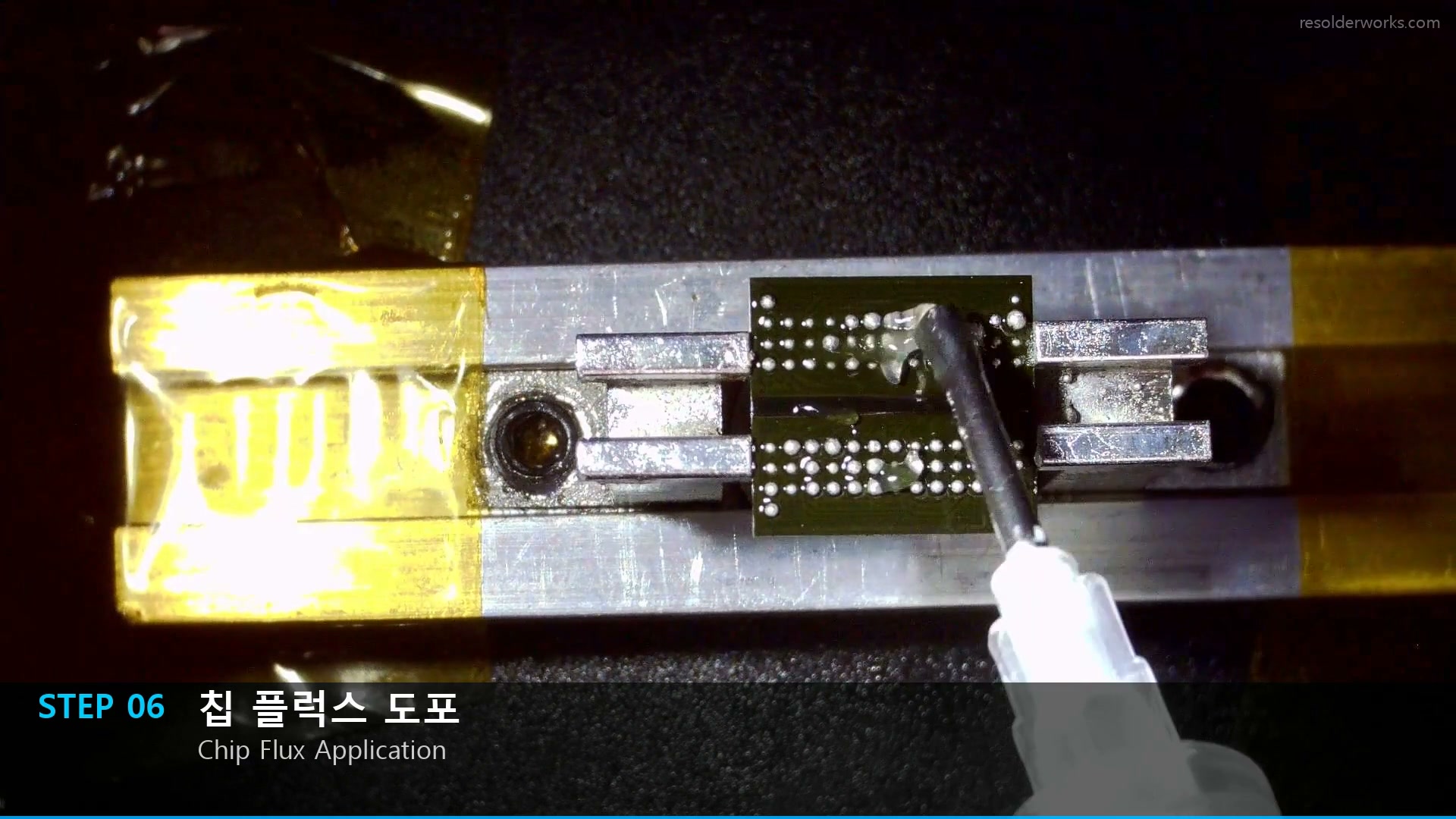 Applying flux to the donor chip's BGA pads
Step 7. Chip Pad Solder Wicking
Residual solder ball material on the donor chip's BGA pads is removed using solder wick. All pads must be flat and clean for the next step — reballing — to proceed correctly.
[Chip pad solder wicking]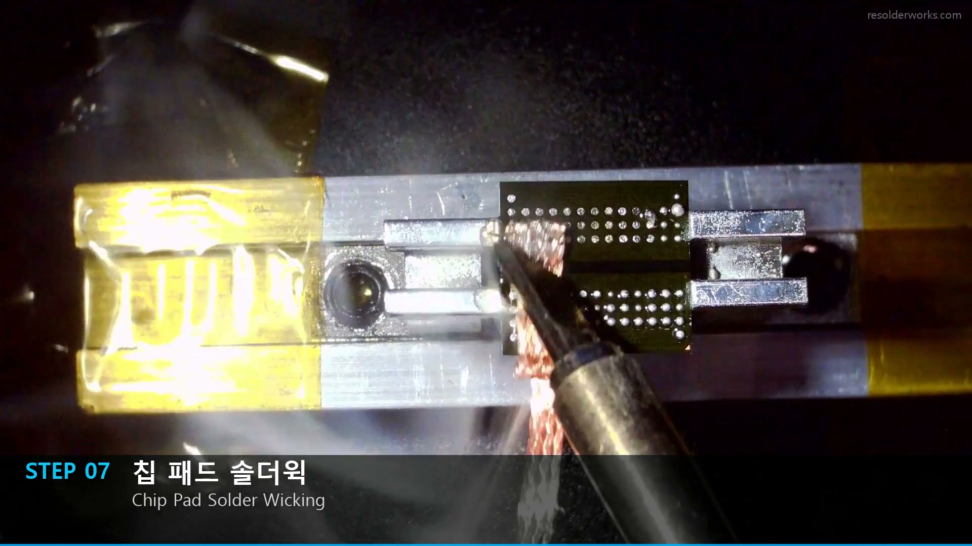 Removing residual solder balls from the donor chip pads
Step 8. BGA Reballing
BGA Reballing is the core process of replacing the solder balls on the underside of the chip. A reballing stencil is aligned to the chip, new solder balls are placed, and heat is applied to form uniform solder balls.
The size and height of each solder ball must be consistent to ensure all pins make reliable contact after mounting.
[BGA reballing]!(/images/uploads/1775127975884-ph5vpp.jpg) Forming new solder balls using a reballing stencil
Step 9. PCB Flux Application
Flux is applied to the PCB pads on the target memory module. This is the final preparation step before chip placement — the right amount of flux helps the solder balls bond properly to the pads.
[PCB flux application]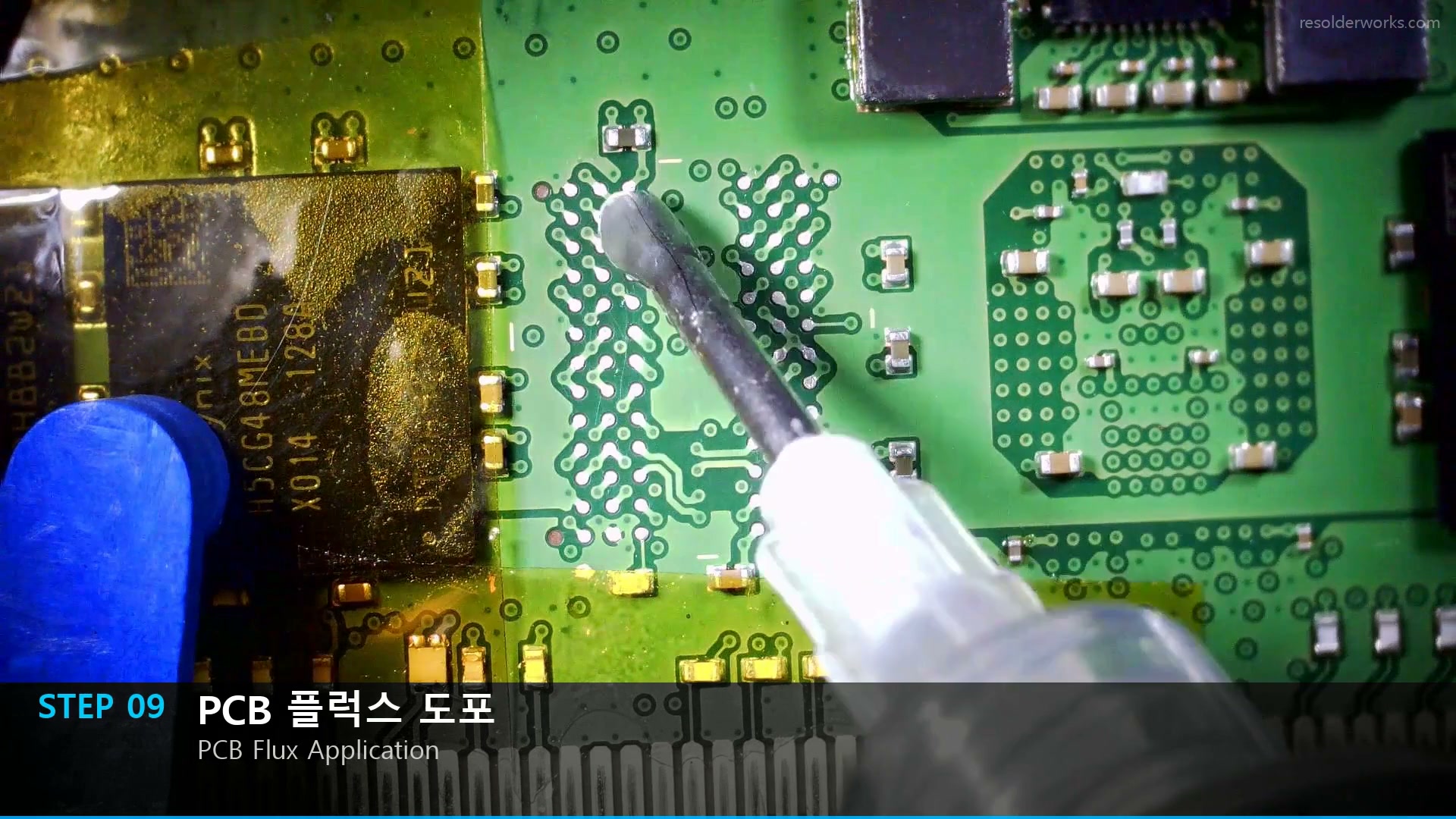 Applying flux to the target PCB pads
Step 10. Donor Chip Placement
The reballed donor chip is placed onto the exact position on the target PCB. We align the chip using the pin 1 marker as reference, ensuring the pads and solder balls line up precisely.
Even the slightest misalignment at this stage can leave some of the hundreds of pins without proper contact, resulting in a failed repair.
[Donor chip placement]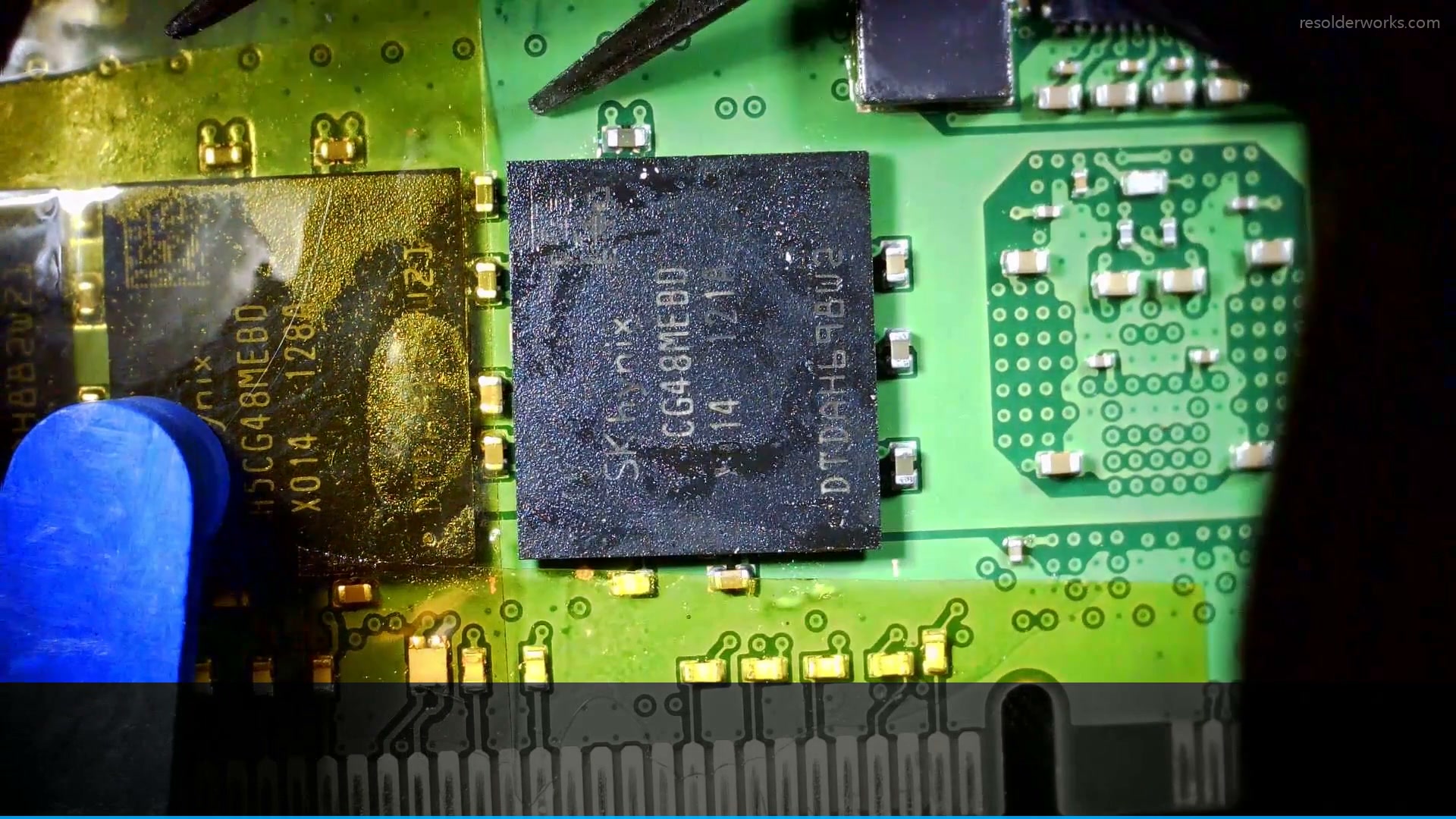 Placing the reballed donor chip onto the target PCB
Step 11. Alignment & Reflow
After confirming the chip's final alignment, we perform reflow using a hot air gun. Following a precise temperature profile — preheat, main heat, and cooling — the solder balls melt and form complete bonds with the PCB pads.
Once reflow is complete, the chip is firmly secured and the BGA rework is finished.
[Alignment and reflow 1]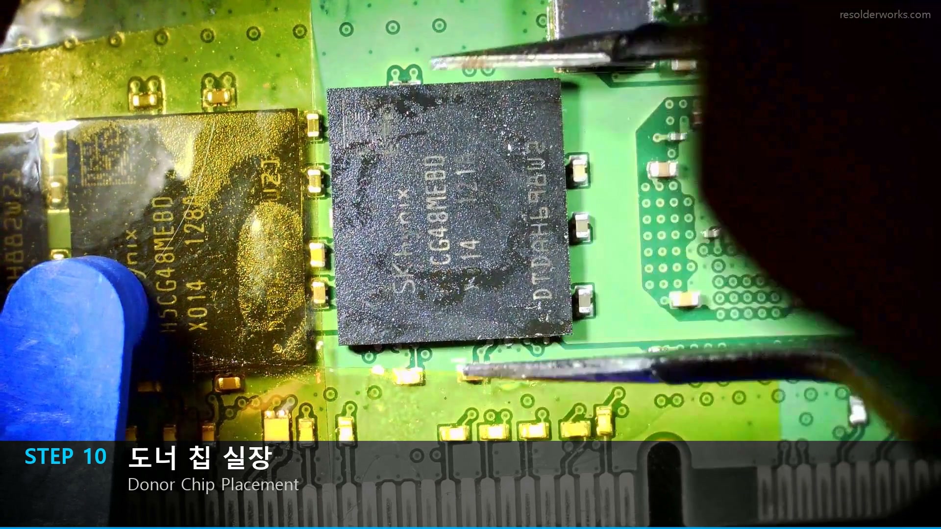 Confirming chip alignment before reflow
[Alignment and reflow 2]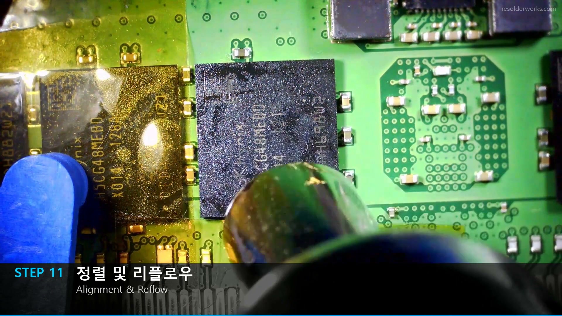 Reflow complete — BGA rework finished
Why Professional BGA Rework Matters
DRAM chip replacement is not simple soldering. Hundreds of microscopic solder balls are arrayed under each BGA-packaged chip, and accurately reballing and mounting them requires specialized equipment and extensive experience.
Without proper BGA rework tools — reballing stencils, hot air guns, preheaters, high-magnification microscopes — the work simply cannot be done. Improper temperature control or alignment errors can cause chip damage, PCB pad delamination, and other problems far worse than the original fault.
ResolderWorks Repair Services
- Server memory DRAM chip replacement (DDR3 / DDR4 / DDR5)
- Professional BGA reballing & rework
- Precision diagnostics with thermal imaging cameras & memory testers
- Bulk repair available for enterprises and data centers
- Full in-house process — from desoldering to reflow
ResolderWorks doesn't just swap parts — we handle the entire process in-house: sourcing components, desoldering, solder wicking, reballing, chip placement, reflow, and final inspection. If you need server memory repair, reach out below.
Need Server Memory Repair?
We specialize in DRAM chip replacement and BGA rework for DDR3 / DDR4 / DDR5 server memory modules. Bulk repair for enterprises and data centers is also available.