How to Find Server Memory Faults with a Multimeter — DDR DRAM Chip-Level Diagnostics Revealed
2026-04-04 · ResolderWorks
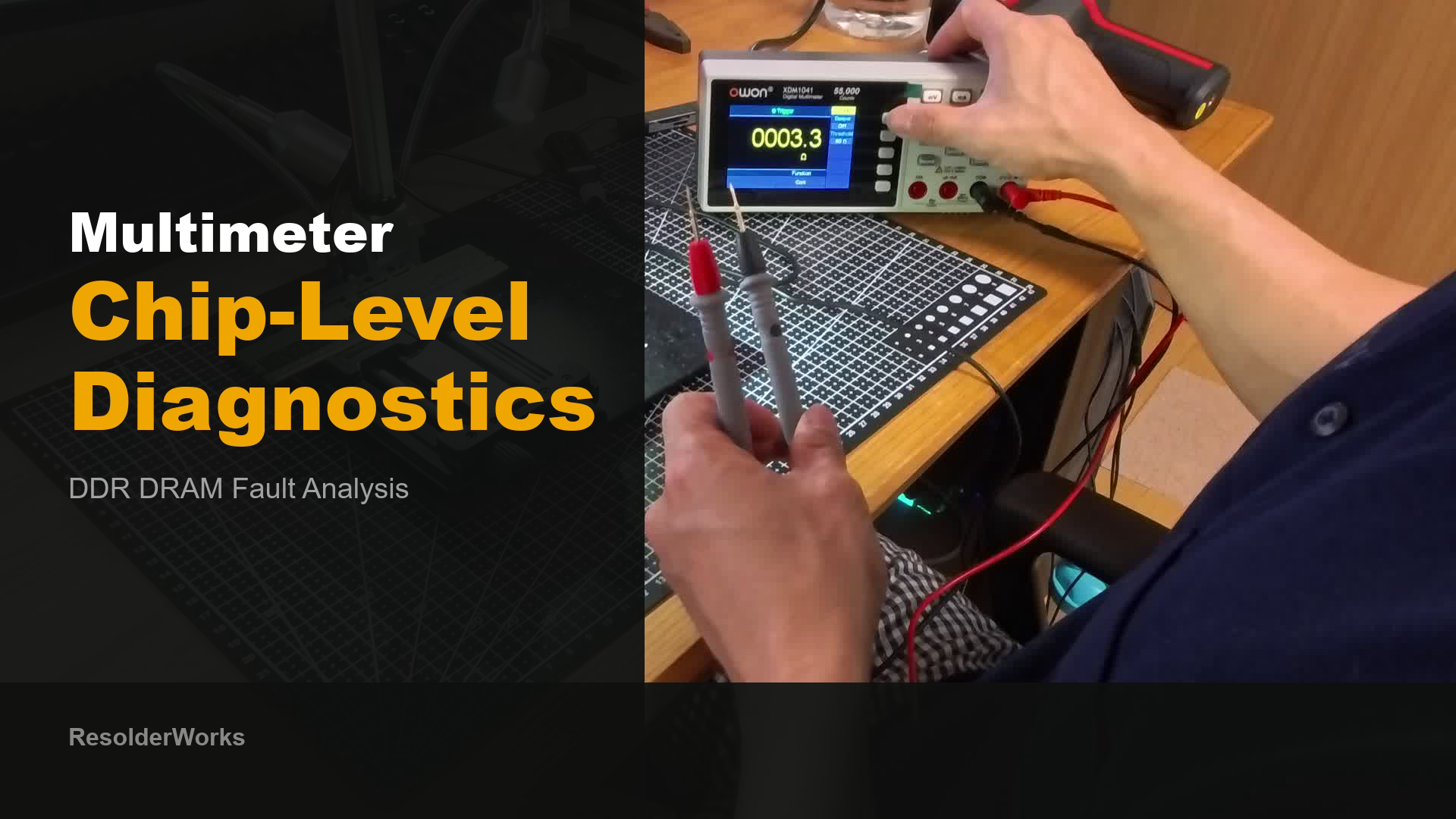
Hello, this is ResolderWorks — a specialist in server memory component-level repair.
Today, we're revealing the multimeter inspection process we actually use to diagnose the root cause of server memory module failures.
A memory tester can tell you "this DIMM is faulty," but it doesn't explain why it's faulty or which pin on which chip is the problem. Without identifying the exact cause before BGA rework, replacing a chip may lead to the same symptoms repeating.
That's why we perform precision multimeter diagnostics before and after every BGA rework.
Step 1. DDR DRAM Pin Map Reference
Before picking up the multimeter, the first thing we do is check the datasheet.
Without knowing the DRAM IC's BGA pin assignment, there's no way to judge whether a reading is normal or abnormal.
[Pin map table]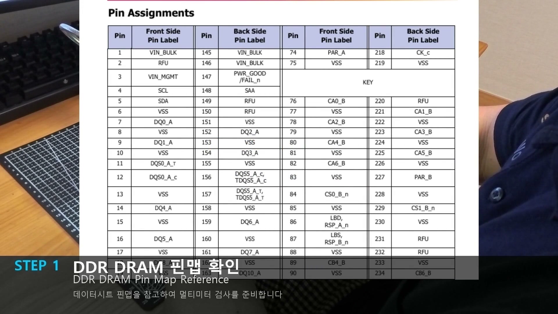 BGA pin map table from the manufacturer's datasheet
[Pin map detail]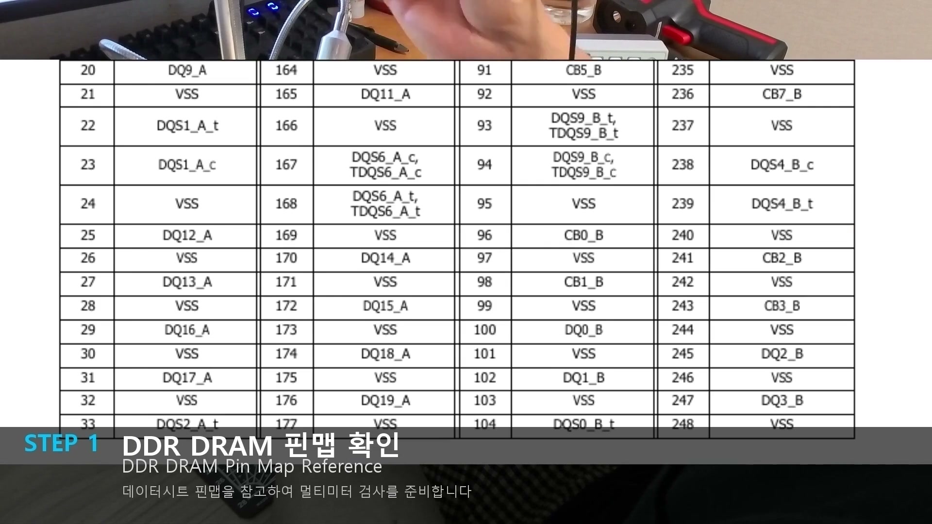 Identifying each pin's function (VDD, VSS, DQ, DQS, CA, etc.)
Why pin maps matter:
- Pin assignments differ by manufacturer — Samsung, SK hynix, and Micron each have different layouts
- DDR4 and DDR5 have completely different pin maps
- Package configurations (x4, x8, x16) also change the layout
- Not knowing NC (No Connect) pins can lead to misdiagnosing normal pins as faulty
Measuring without a pin map is like driving blindfolded.
Step 2. Diode Mode Test
With the pin map ready, we begin the first hands-on measurement: diode mode testing.
DRAM IC I/O pins have built-in ESD protection diodes. Using the multimeter's diode mode, we apply a small voltage to each BGA ball and read the forward voltage drop across the internal PN junction.
[Diode mode test]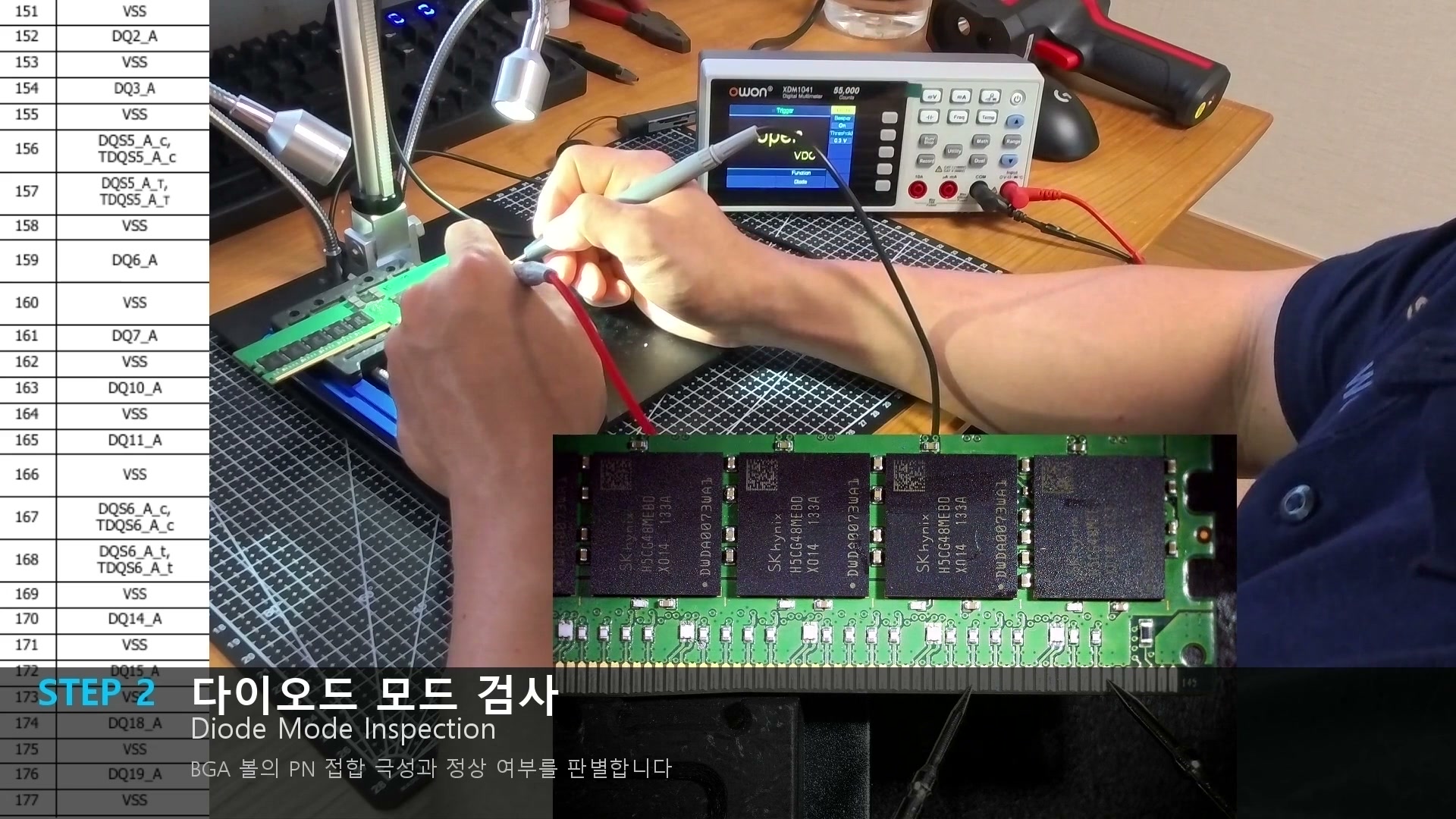 Testing BGA balls in multimeter diode mode
[Diode probing]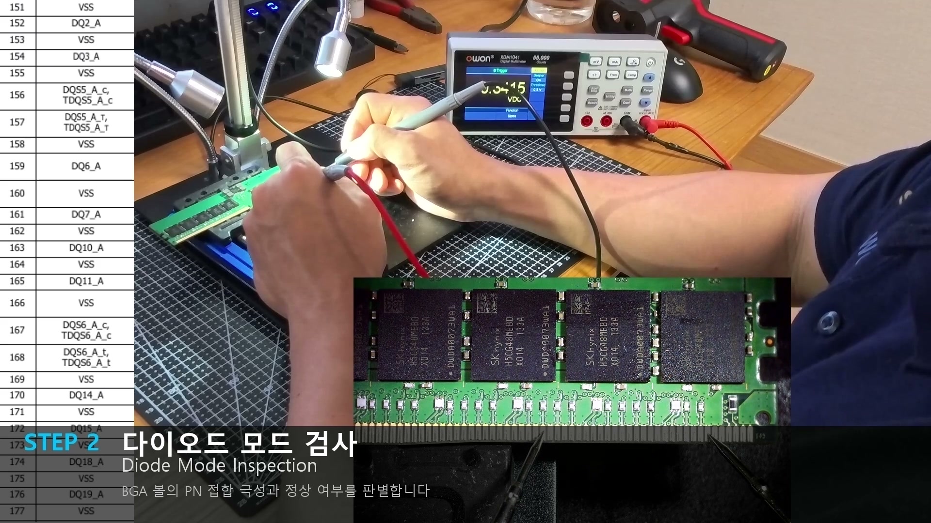 Measuring forward voltage drop on each pin
What this test reveals:
| Reading | Meaning | |---------|---------| | 0.3–0.7V | Normal — internal PN junction healthy | | ~0V | Suspected short — pin-to-pin or pin-to-GND | | OL (Over Limit) | Open — bond wire break or die damage |
All DQ pins in the same byte lane should show nearly identical diode values. If seven pins read 0.5V but one reads OL, that pin's bond wire or die connection is broken.
This single test can catch dead chips, ESD damage, and solder bridges. It takes roughly 2 minutes per IC.
Step 3. Resistance Measurement
The second hands-on measurement uses resistance mode. We measure the resistance from each BGA ball to its destination — via, termination resistor, or memory controller pin.
[Resistance measurement]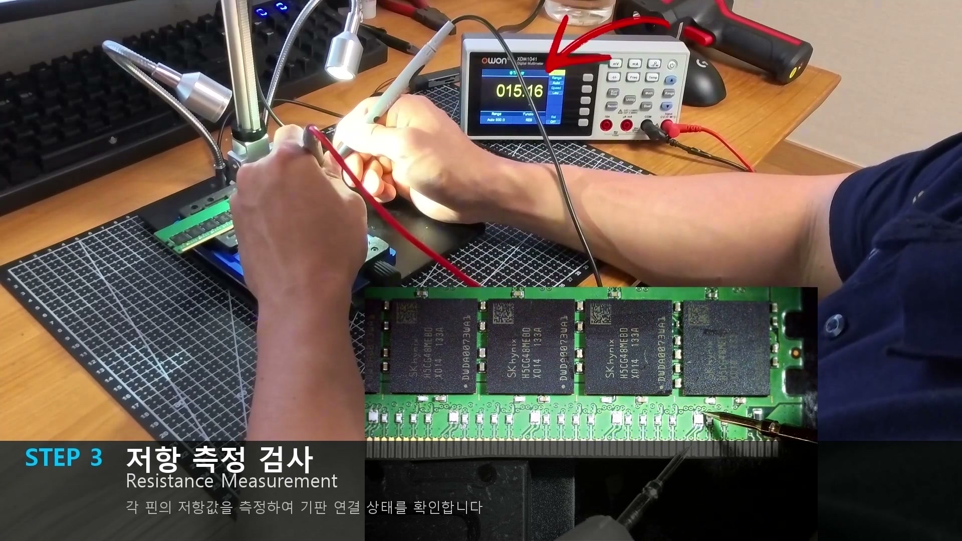 OWON multimeter showing 015.16Ω
[Resistance overload]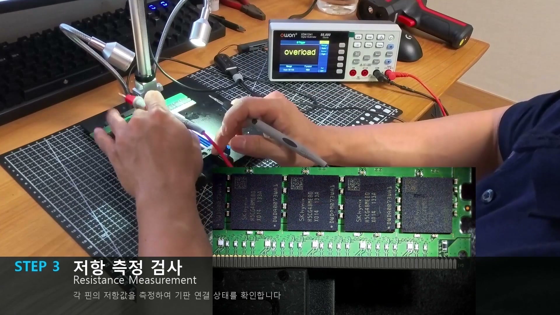 "Overload" display — path is open or beyond measurement range
An "overload" reading means the path is completely open or exceeds the measurement range. We cross-reference with the pin map to determine whether it's an NC pin or an actual break.
[Resistance reading]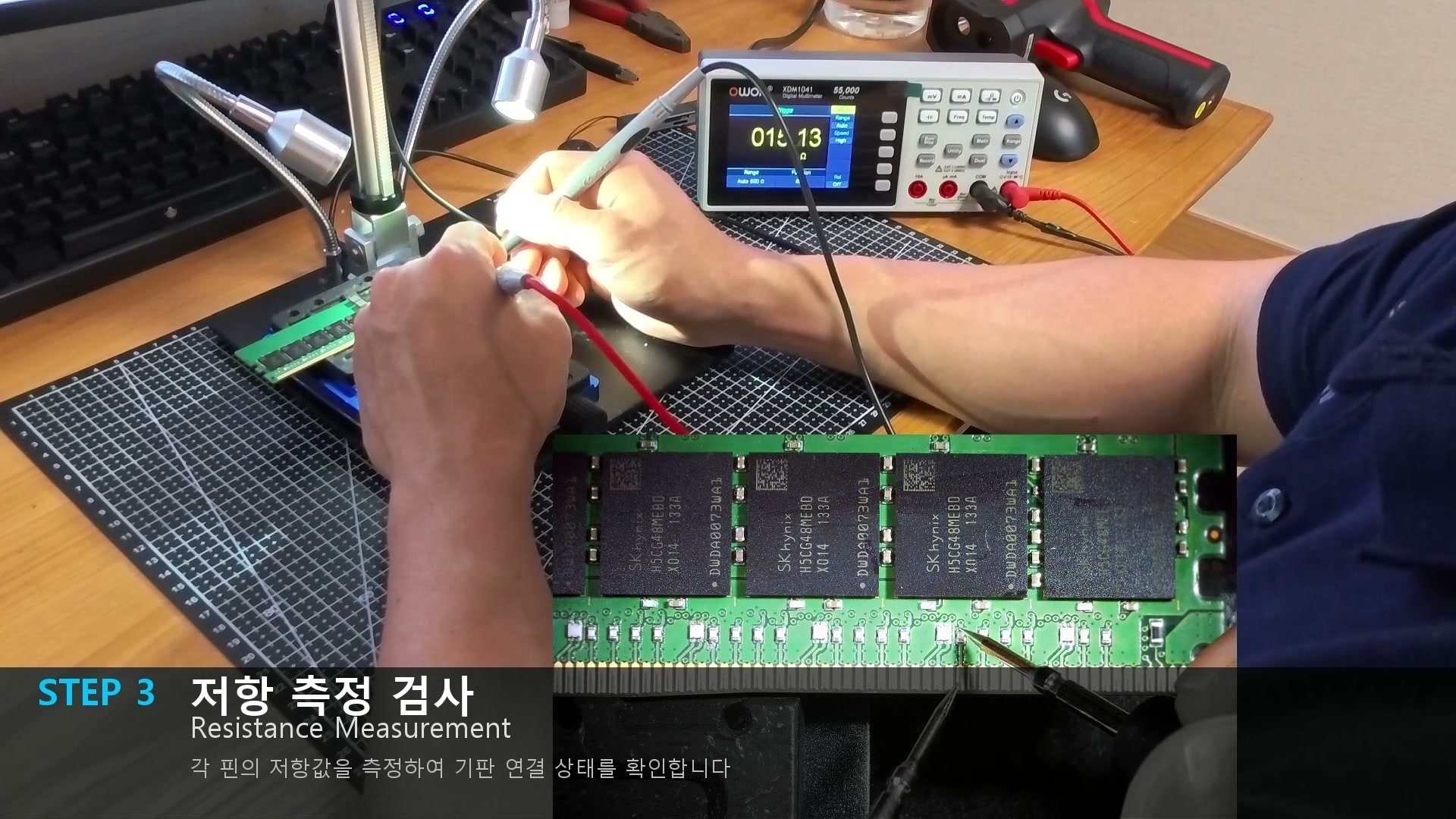 Checking resistance values pin by pin
Key points for resistance measurement:
- Power rails (VDD, VSS): All pins in the same group must show very low, uniform resistance. If one is high, that ball's solder joint is defective.
- Data line uniformity: DQ0 through DQ7 should all fall within a similar range. One outlier means that joint is the problem.
[15kΩ reading]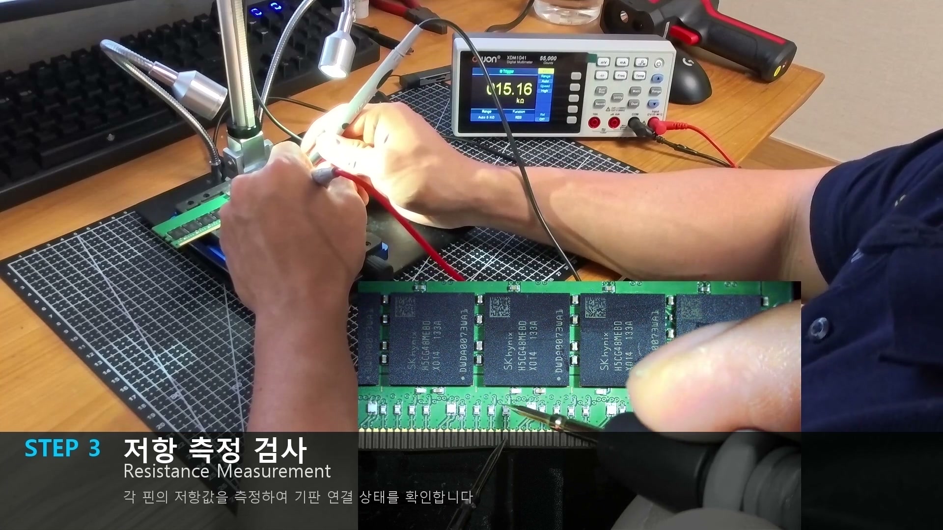 15kΩ measurement
[28kΩ reading]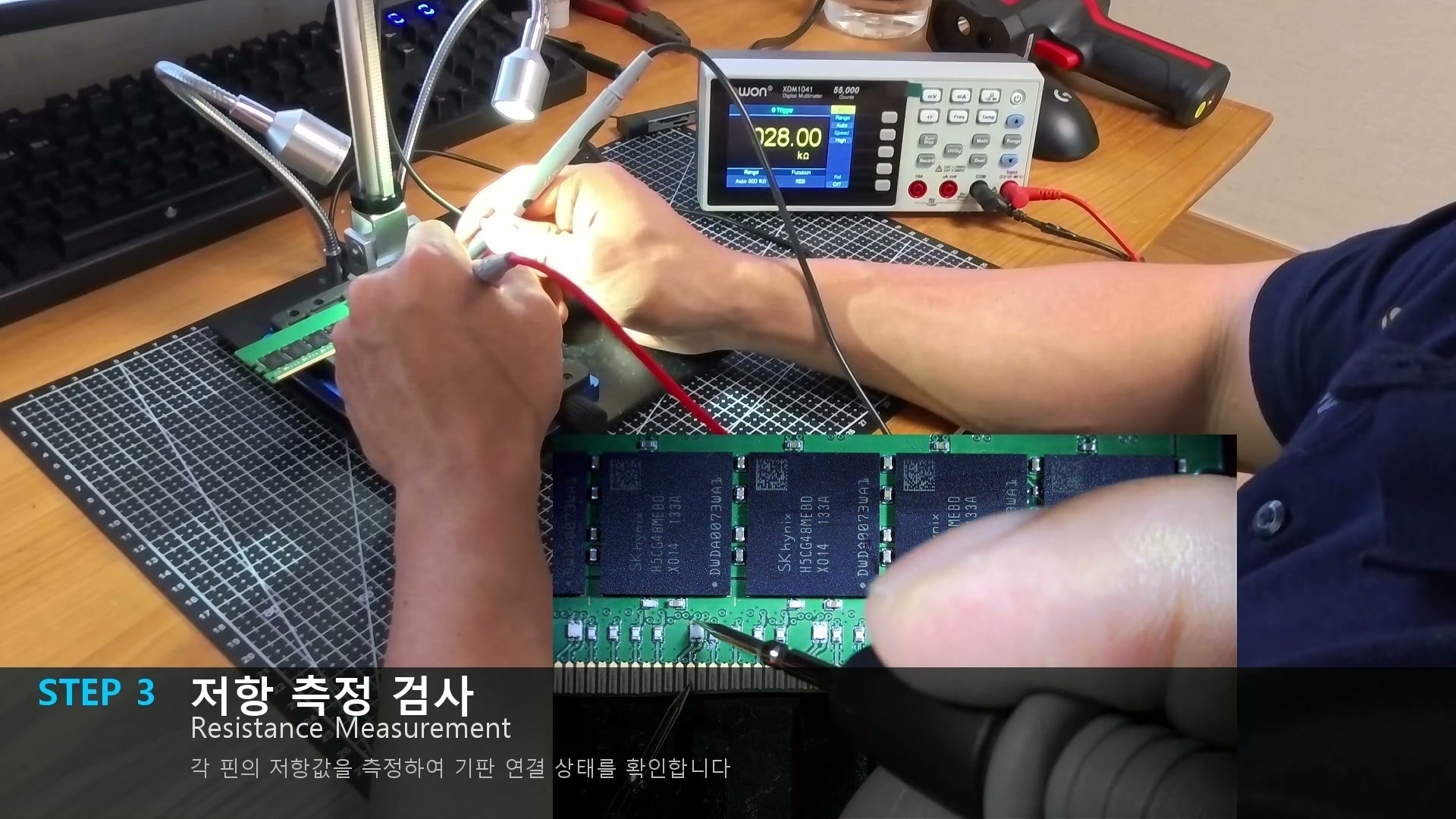 28kΩ measurement
The absolute value matters less than uniformity across pins with the same function.
Even after rework, a joint that looks fine visually may actually have high resistance. It might pass a quick memory test but fail under sustained load. Resistance measurement catches these latent defects before they cause problems.
Step 4. Continuity Test
The final step is the continuity test — the simplest but fastest inspection method. The multimeter passes a small current and beeps if resistance falls below a threshold (typically 30Ω).
[Continuity test open]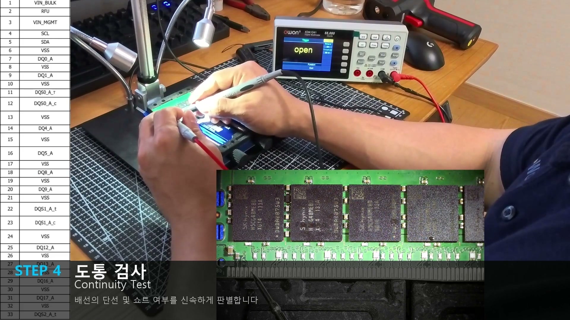 "Open" display — this line is not connected
When "open" appears, we cross-reference the pin map to determine whether the pin is supposed to be NC or if it's an actual break.
[Continuity voltage]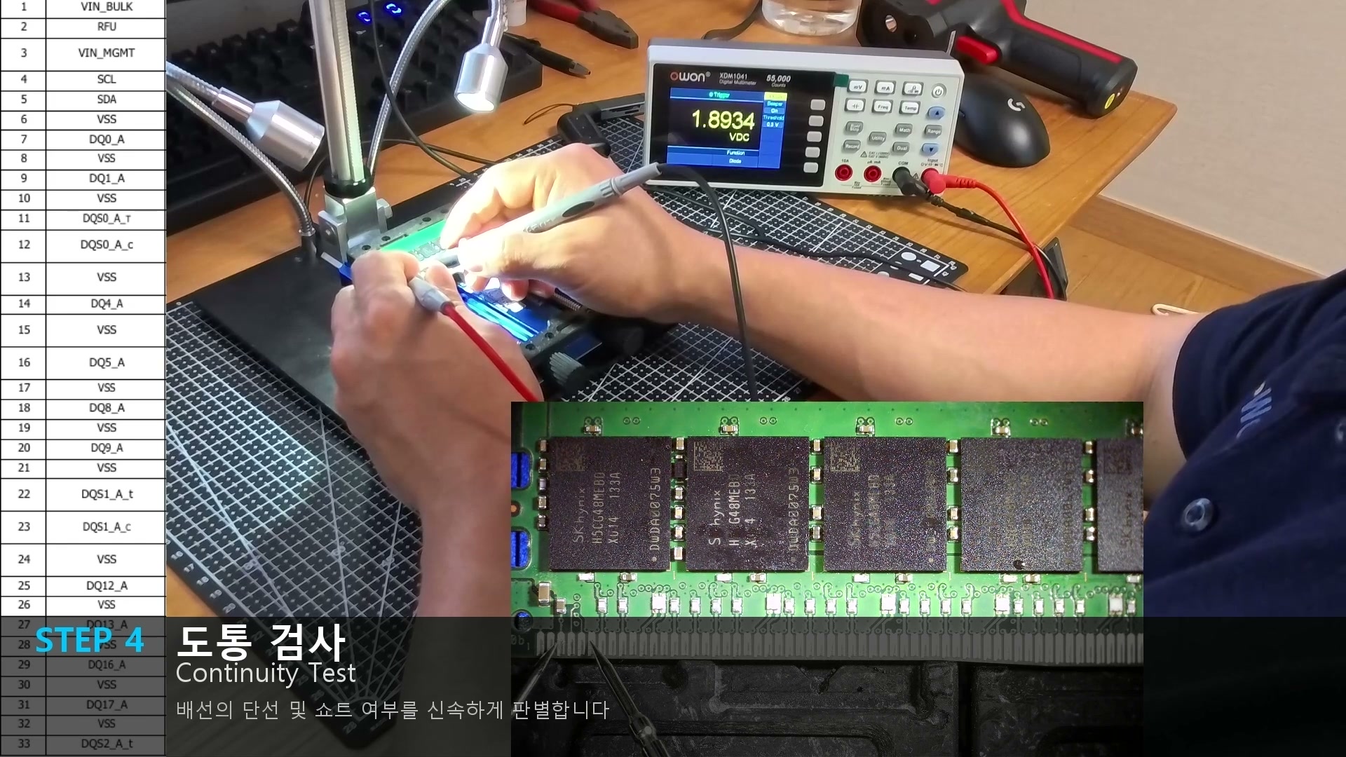 1.8934V displayed — normal or abnormal depends on pin function
[Continuity probing]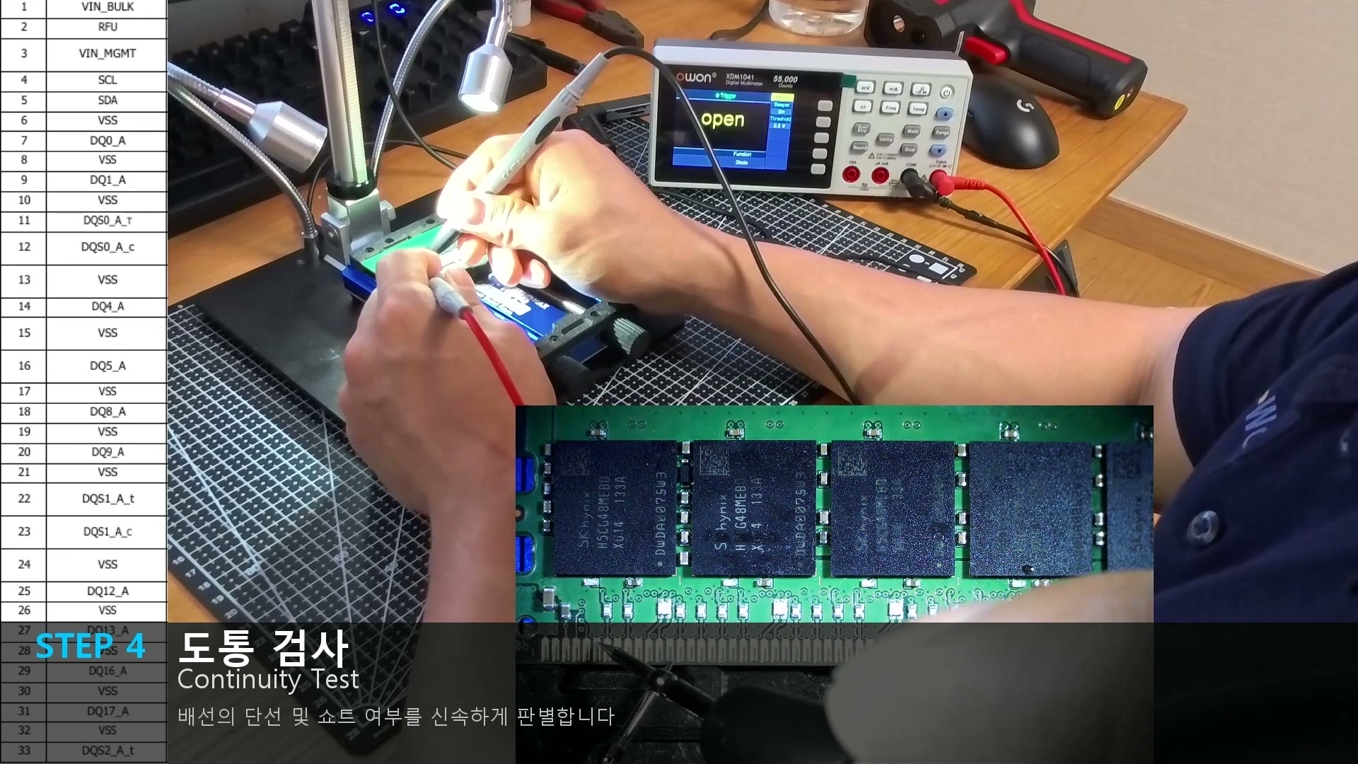 Verifying the complete signal path from BGA ball to edge connector
What we focus on during continuity testing:
- Power rail continuity: All VDD pins must be connected to each other. Same for VSS. If even one fails, that ball is open.
- Pin-to-pin short detection: A beep between pins that shouldn't be connected means solder bridge.
- Via integrity: Server memory PCBs are multi-layer boards. A signal path passes through 4–6 vias from BGA pad to destination — a crack in any one breaks continuity.
- End-to-end verification: We verify the full signal path from the DRAM ball to the edge connector pin.
The most common defect after BGA rework is a solder bridge — continuity testing catches it in seconds.
Summary: The Multimeter Diagnostic Pipeline
At ResolderWorks, every BGA rework follows this sequence:
Pin Map Reference → Diode Test → Resistance Measurement → Continuity Test
Performing these four steps before and after rework systematically answers:
- Diode test: Is the chip alive?
- Resistance: Are the solder joints healthy?
- Continuity: Is the wiring intact?
With a $200 multimeter and a datasheet, you can find the answer to "why is it faulty" — something a $20,000 memory tester can't explain.
ResolderWorks Repair Services
- Server memory repair (DDR3 / DDR4 / DDR5)
- DRAM and PMIC chip replacement, BGA rework & reballing
- Precision diagnostics with multimeter, memory tester & thermal camera
- Bulk repair available for enterprises and data centers
- Full in-house process — from diagnostics to rework to verification
Need Server Memory Repair?
[Contact]
We specialize in DRAM chip replacement and BGA rework for DDR3 / DDR4 / DDR5 server memory modules. Bulk repair for enterprises and data centers is also available.